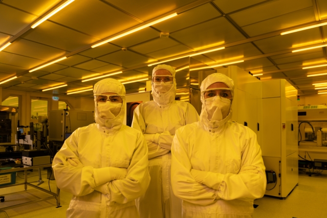
Permanent bonding solutions
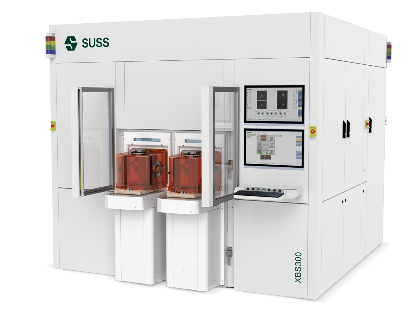
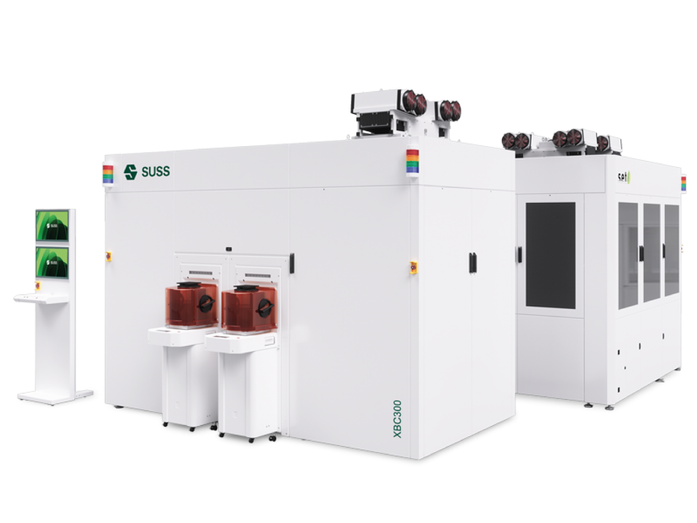
XBC300 Gen2 D2W ​ Wafer Bonder

Increase production capacity, minimize yield losses: XBC300 Gen2 D2W platform is your fully automated solution for sequential die-to-wafer hybrid bonding on 200mm and 300mm substrates. 

3DREND~2.PNG

Creating bonds you can rely on

The XBC300 Gen2 D2W combines industry-leading precision with maximized throughput and significantly reduced yield losses. The integrated platform includes all process steps—particularly surface activation and die positioning—in a single, fully automated solution.​​ All this in a footprint that’s unmatched in the market. 

Ultra-High Accuracy

With an alignment accuracy of +/- 100nm, the XBC300 Gen2 D2W has been specifically developed to meet the particular requirements of advanced 3D IC architecture, especially for high-bandwidth memory applications. 

Industry-Leading Footprint

Measuring 3.12 m wide and 4.4 m long, the footprint of the XBC300 Gen2 D2W is up to 40% smaller than any comparable system on the market. 

State-of-the-Art Performance

The XBC300 Gen2 D2W wafer bonder enables high-speed production with an alignment accuracy of ±100 nm. This impressive precision is achieved through the integration of the NEO HB flip-chip die bonding platform—developed by our technology partner, SET Corporation SA—with SUSS modules for cleaning, surface activation, and metrology.

Integrated In-Situ Metrology

Equipped with a high-precision, throughput-optimized metrology station, the XBC300 Gen2 D2W enables in-line verification of alignment accuracy for D2W bonds throughout all process steps. The metrology module supports full-field IR overlay measurement and IR void inspection, with a detection resolution above 500 µm.

Die-to-Wafer hybrid bonding solution for global production and R&D

Key Features of XBC300 Gen2 D2W ​Wafer Bonder

Developed in collaboration with our technology partner SET Corporation SA, the XBC300 Gen2 D2W is particularly suited for the needs of R&D lines, research and technology organizations (RTOs), as well as low volume manufacturing (LVM). 

Up to 1,000 dph


The integrated NEO HB flip-chip die bonder enables high throughput with significantly reduced yield losses. ​This flexible system supports die sizes ranging from 1×1 mm to 22×22 mm and accommodates 200/300 mm wafers as well as 400 mm tape frames. 

DSC00170_highRes.jpg
< 40 µm Inter-Die Spacing

The XBC300 Gen2 D2W wafer bonder allows for high die densities on target substrates when needed, enabling you to achieve minimal voids for maximum yield. 

D​ie Handling Down to 30 µm

Based on the industry-renowned XBC300 Gen2 platform, the XBC300 Gen2 D2W allows for the handling of even extremely thin microchips on tape frame carriers.

Downloads

Looking for more details? Please click below to download the technical datasheet and our product presentation with in-depth product information.

Related products

Discover our portfolio of permanent bonding solutions

XBS300 W2W

XBS300 W2W hybrid bonding platform is designed for automated hybrid fusion bonding of aligned 200mm and 300mm wafers.
Learn More
Automated

XBC300 Gen2 D2W/W2W

Hybrid bonding platform that integrates W2W, collective D2W, and sequential D2W bonding in a single system.
Learn More
XBC300~1.PNG
Automated