Uniform UV exposure for consistent results
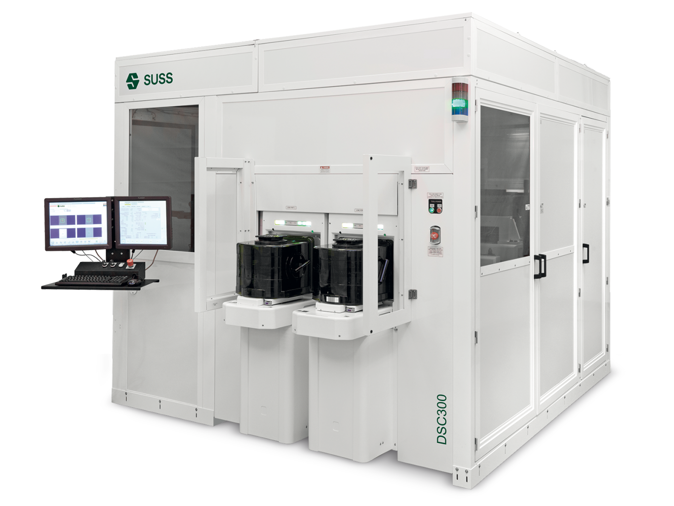
SUSS Projection Scanner
SUSS Projection Scanner deliver a unique projection lithography solution for advanced wafer processing. Combining full-field UV exposure with single continuous scanning, they ensure uniform results without stitching or over-exposure defects. Designed for high throughput and non-contact operation, our systems enable cost-efficient, high-resolution lithography across diverse applications in semiconductors, MEMS, and advanced packaging.