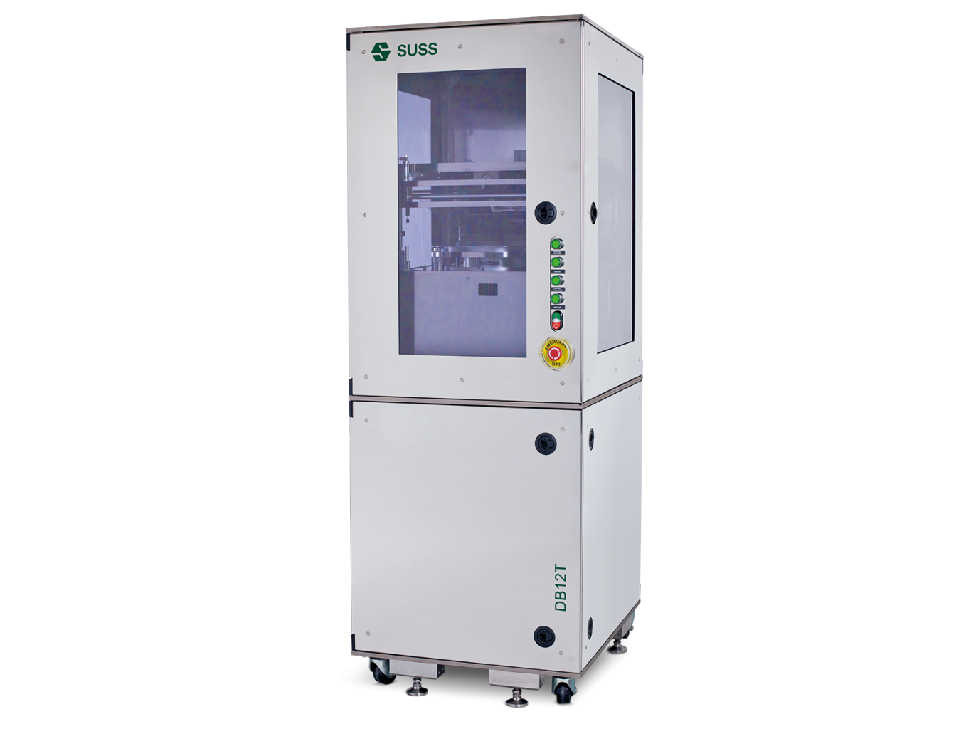
DB12T Debonder

Mechanical Peel-off Debonder

The DB12T debonder represents the state-of-the-art solution for mechanical peel-off debonding at room temperature for a large variety of thin wafer handling applications. These applications include power devices, 2.5D interposers and 3D integrated devices as well as 3D wafer level packaged MEMS, fan-out wafer-level packages and others.

While granting full control over the debond front propagation, DB12T debonds the support carrier from tape mounted thin wafers as thin as 50 μm or even below. It is compatible with the largest choice of adhesives and release layers that have been designed for mechanical debonding. Tooling options for wafer sizes ranging from 4" to 12" and different carrier materials such as glass or silicon are available for the DB12T debonder.

Highlights

  • Shortest possible debond front
  • Compatible with largest choice of adhesive systems for mechanical debonding
  • High throughput processing
  • Advanced process control

Prior to mechanical peel-off debonding on the DB12T, the bonded wafer stack needs to be mounted on a tape frame using standard tape mounting equipment. The DB12T debonder uses a porous chuck to hold the tape mounted wafers flat and in place. The wafer stack is mounted in a way that the thin wafer is on the tape side which is held by the porous vacuum chuck. The carrier is facing a flexible plate which is attached to the top side of the carrier for debonding.

To start the mechanical separation process, a debond initiator blade is inserted underneath the carrier from one side. The insertion height can be controlled with micrometer precision. Different initiator blades are available depending on the combination of carrier and device wafer. When the flexible plate is lifted from one side, a programmable roller is used to control the flex of the plate and carrier as well as the propagation of the debond front throughout the entire separation process. The roller ensures the shortest possible debond front across the wafers. This way the mechanical stress on the device wafer is kept at a minimum.

The DB12T can be computer controlled and all relevant debond parameters are either adjustable or recipe programmable in order to ensure optimum debonding performance for different wafer sizes and topography. Interlock parameters are available in the recipe which stop the separation process if the debond front is not propagating in order to ensure thin wafer integrity.

A fully automatic operation, including substrate handling and carrier removal, is supported by integrating the mechanical peel-off debonder module DB300T which is based on the DB12T into the XBC300 Gen2 debonder.