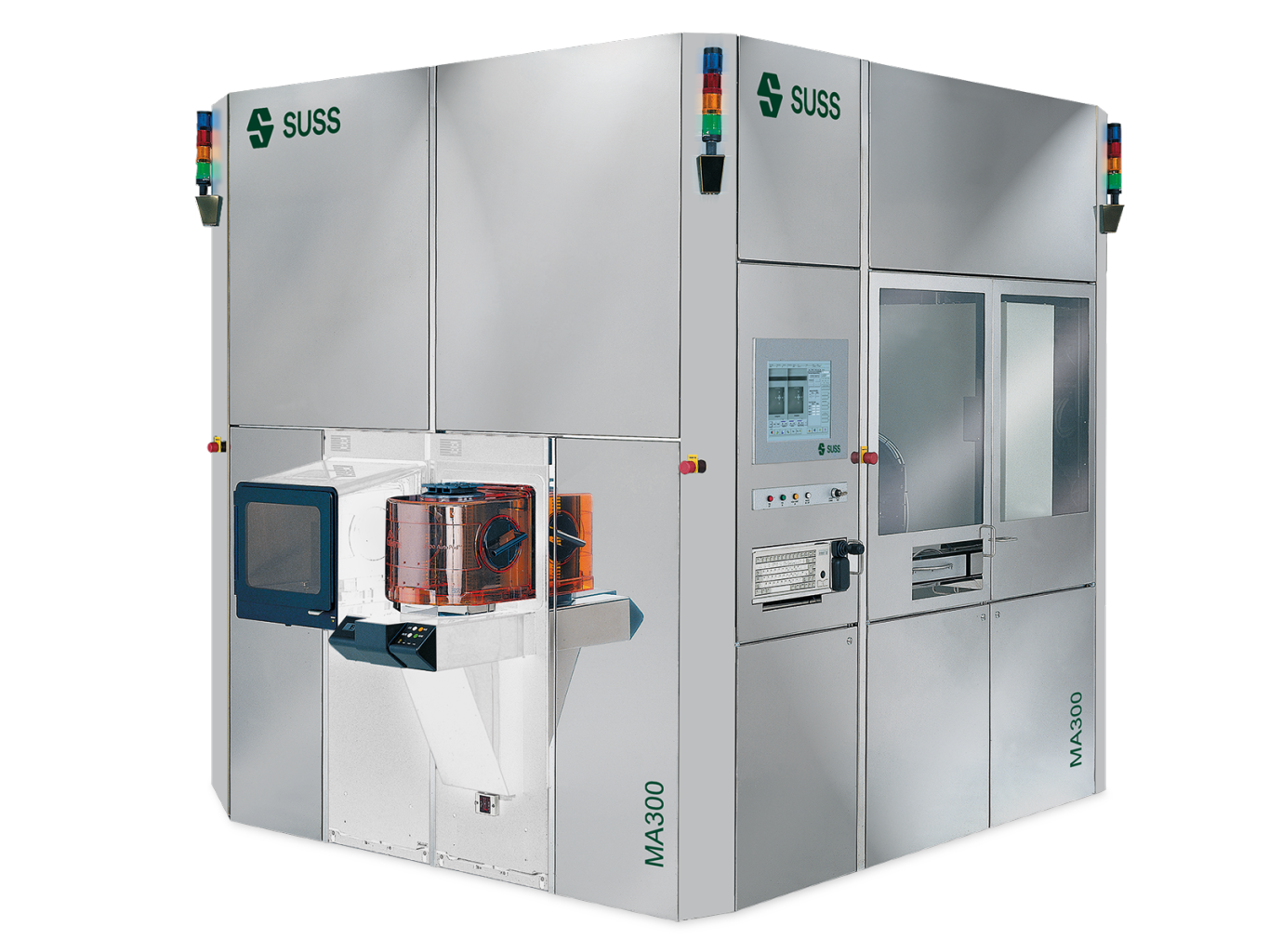
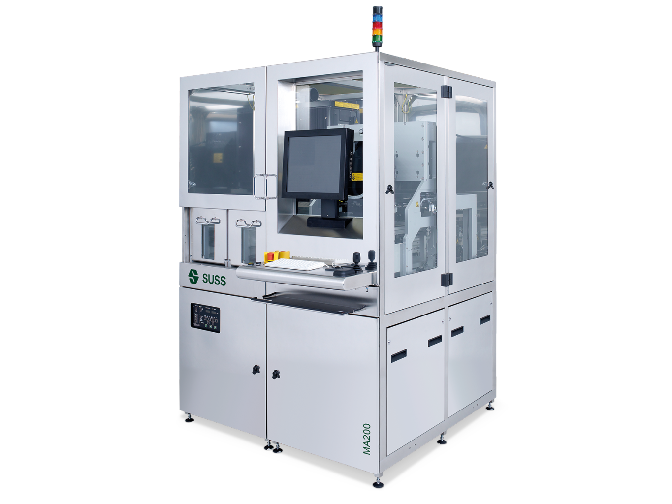
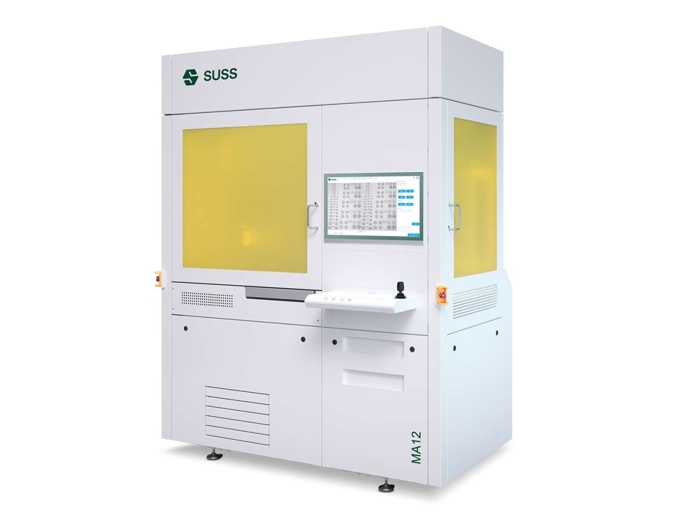
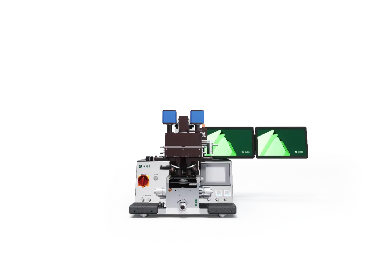
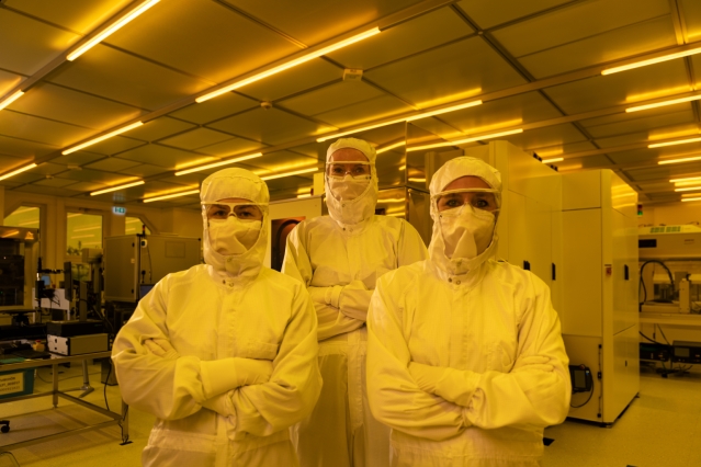
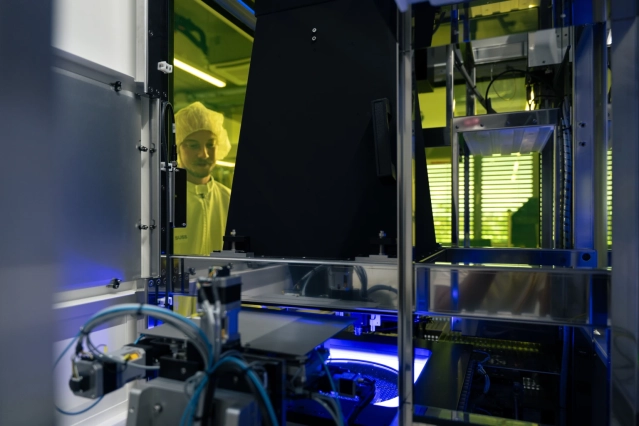
Reliable mask alignment under all conditions
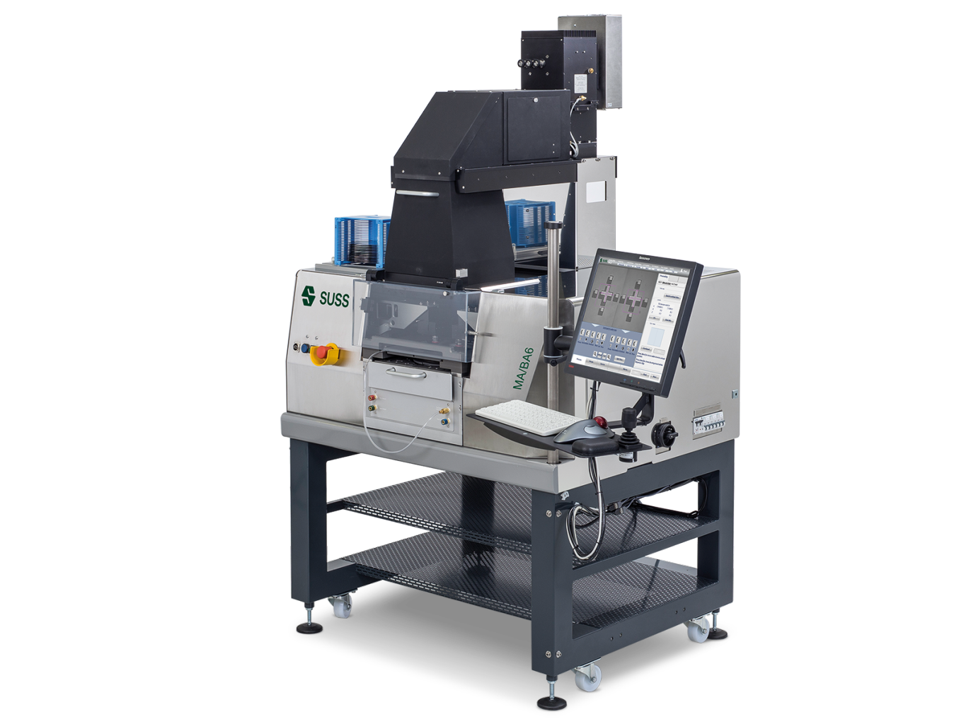
Mask Alignment
SUSS Mask Aligners combine superior alignment accuracy with advanced exposure optics to meet the toughest lithography challenges. Designed for substrates up to 300 mm, they deliver stable overlay, high yield, and reliable results across diverse applications for any scale – from R&D to high-volume manufacturing.