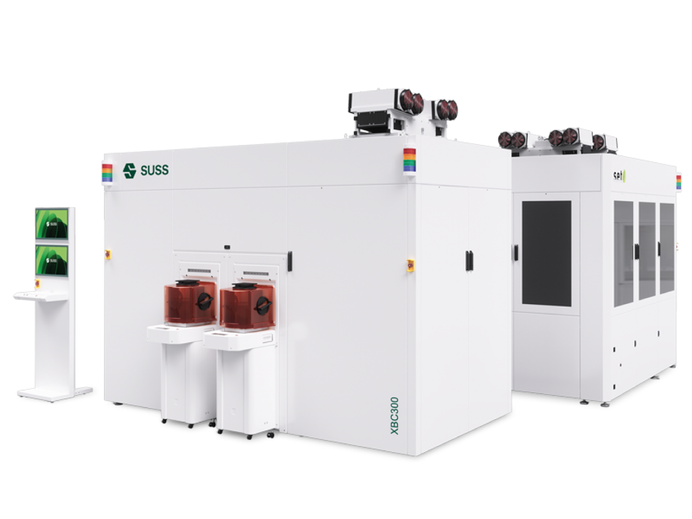
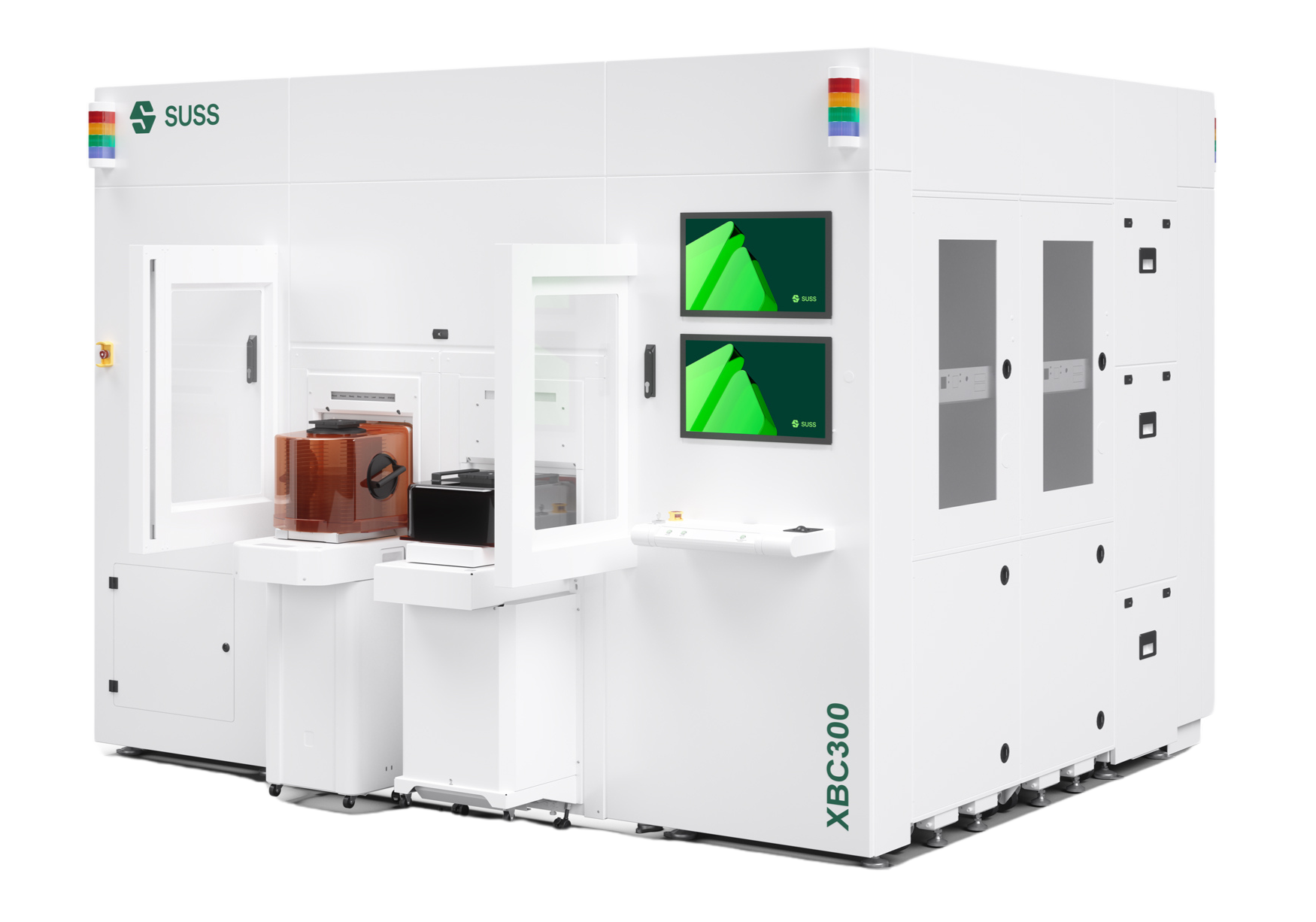
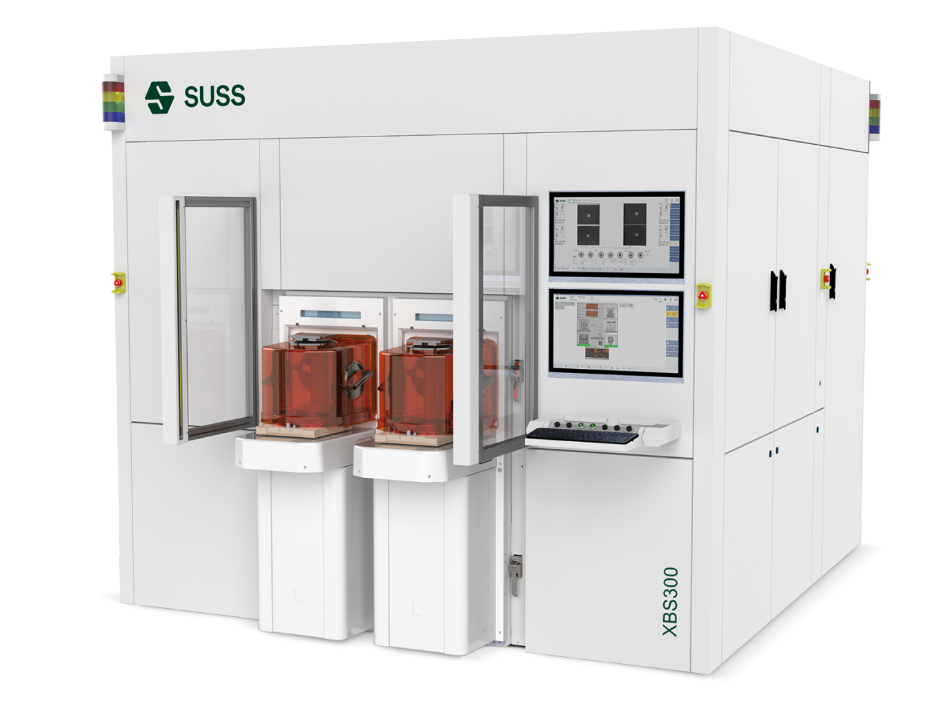
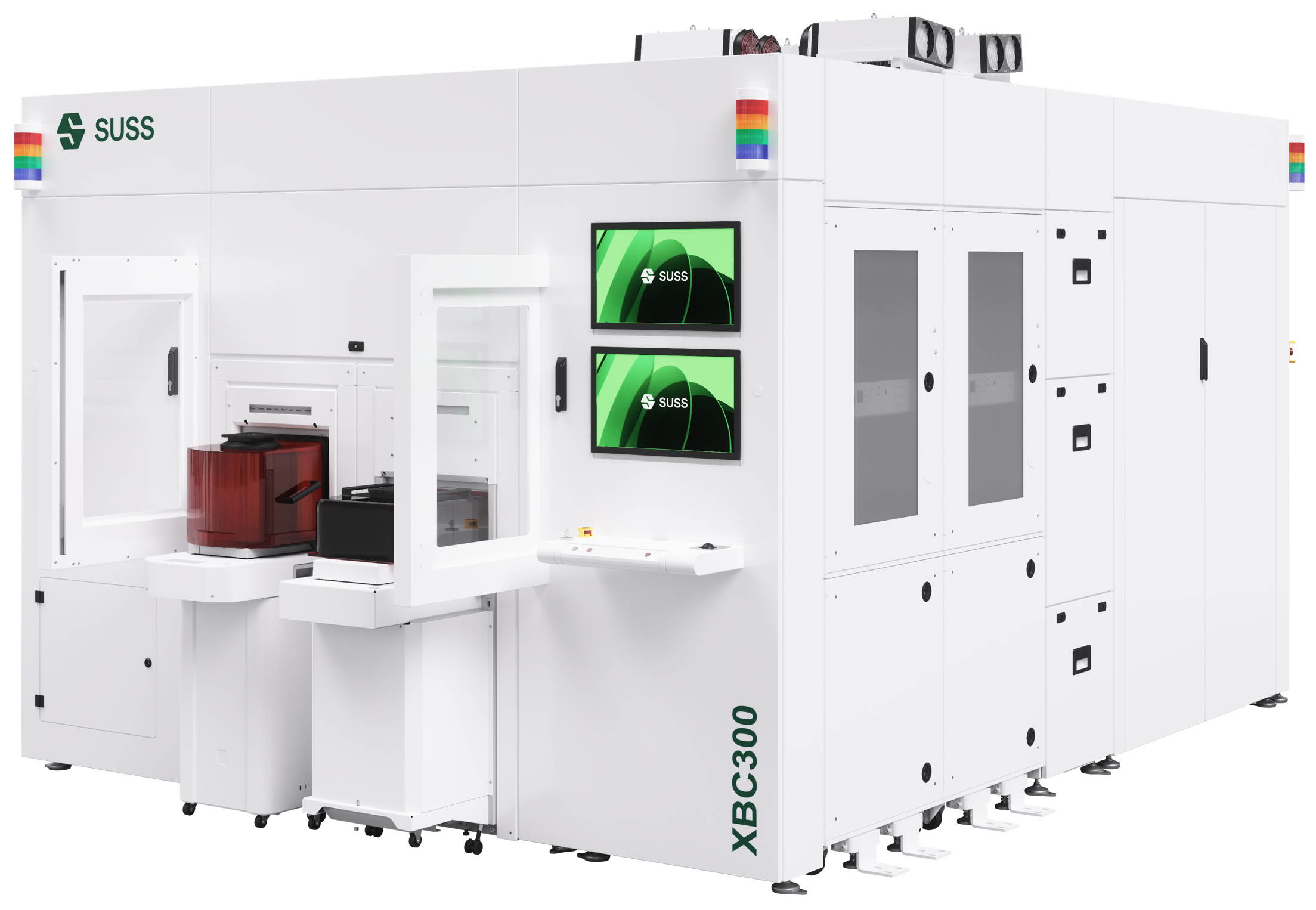
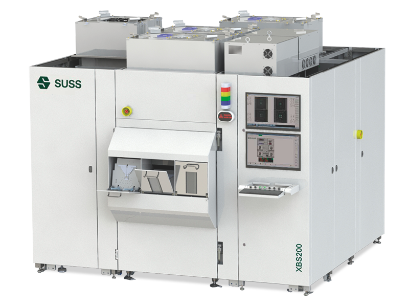
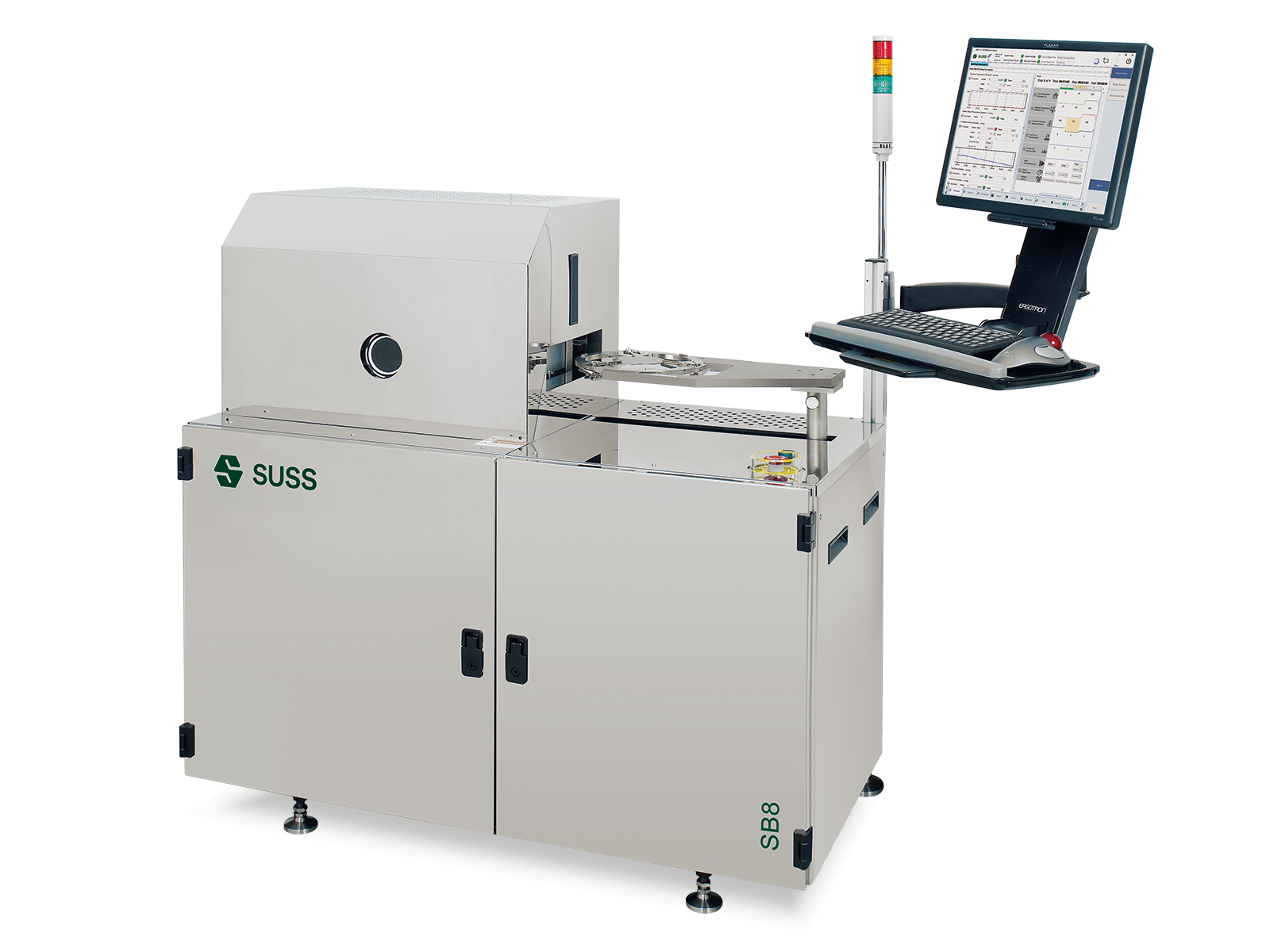
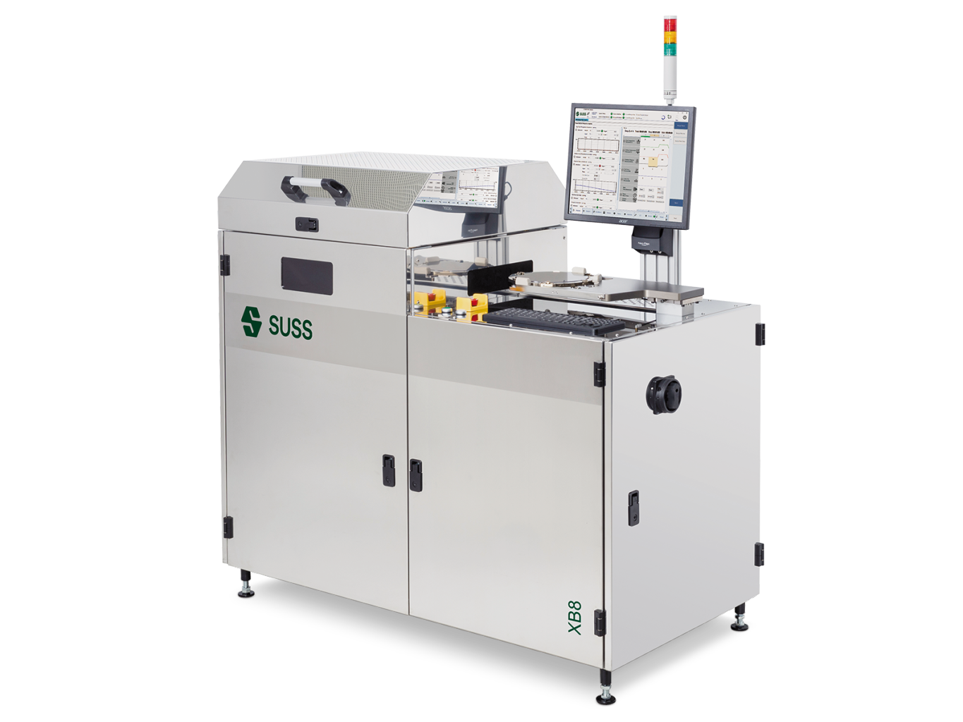
- Automated
- Semi-Automated
- Manual
- Automated
- Semi-Automated
- Manual
- Automated
- Automated
- Semi-automated
- Automated
The bond aligner BA Gen4 is designed for manual alignment and subsequent bonding of substrates up to 200 mm in size. Further functionality becomes available after the optional addition of mask aligner tooling. The BA Gen4 series is utilized in advanced packaging, MEMS production and whenever sub-micron precise alignment and high precision repeatability are required.
Excellent alignment accuracy
Low cost of ownership
Easy system expansion
The alignment process from wafer to wafer on the BA Gen4 Series is based on the same high-performance technology which has proven itself in the SUSS MicroTec mask aligners for aligning masks to wafers. With fusion bonding of silicon substrates the BA Gen4 series offers additional functionality. Available for further bonding operations: the SUSS MicroTec manual bonder SB6/8 Gen2. A special BA Gen4 fixture system ensures reliable transport of the wafer package.
The manual operation of the BA Gen4 series and the easy switch between options allows the operator to be highly flexible for applications in the most wide-ranging research and development processes. The choice of possible alignment operations allows a wide range of process requirements to be covered. The operator is supported by automated features such as on-screen structure visualizations and automatic wedge error compensation.
Top-Side Alignment (TSA)
Where lithographic processes require the alignment of structures on only one side of the device wafer (e.g. RDL, micro-bumping and similar techniques), top-side alignment is used to align the fiducials on the mask with those of the wafer. Depending on the substrate properties, this can be achieved either using stored position data for the wafer or through live image alignment, as with the DirectAlign® system invented by SUSS MicroTec.
Highlights
Available for:
Automated Mask Aligner
Semi-Automated Mask Aligner
Manual Mask Aligner
Bottom-side Alignment (BSA)
Alignment of the structuring on the wafer back side with the structures on the front is required in processes in the field of MEMS, wafer-level packaging, 3D integration and imprint applications. Optical bottom-side alignment is normally used for this type of alignment. An integrated camera system detects the mask or stamp structures and the structures on the substrate back side, and aligns them with each other. The substrate position must be determined and stored prior to loading, since the substrate subsequently covers the mask target. This places specialized demands on the alignment system as a whole.
Highlights
• With its outstanding level of mechanical precision and stability, the SUSS mask aligner offers unmatched accuracy
Available for:
Automated Mask Aligner
Semi-Automated Mask Aligner
Manual Mask Aligner
Infrared Alignment
Multilayer wafer stacks are used in a number of structuring processes. The alignment marks that are normally embedded between the layers can be identified and aligned via infrared (IR) illumination. This requires the use of materials that are transparent for IR light, such as undoped silicon, III-V semiconductors (e.g. GaAs) and adhesives for temporary bonding and debonding techniques.
The SUSS equipment can be optionally equipped with powerful IR light sources and high-performance camera systems, ensuring optimal IR availability.
Highlights
Available for:
Automated Mask Aligner
Semi-Automated Mask Aligner
Manual Mask Aligner
Fusion bonding refers to the spontaneous adhesion of two planar substrates with a dielectric material (typically silicon oxide) as the bonding layer. The process usually involves a proper surface activation that renders the substrates largely hydrophilic. Subsequently, the substrates are aligned, brought into contact and finally tempered at elevated temperature.
Available for:
Automated Bonder
Semi-Automated Bonder
Semi-Automated Bond Aligner
Semi-Automated Mask and Bond Aligner
Infrared Alignment
Multilayer wafer stacks are used in a number of structuring processes. The alignment marks that are normally embedded between the layers can be identified and aligned via infrared (IR) illumination. This requires the use of materials that are transparent for IR light, such as undoped silicon, III-V semiconductors (e.g. GaAs) and adhesives for temporary bonding and debonding techniques.
The SUSS equipment can be optionally equipped with powerful IR light sources and high-performance camera systems, ensuring optimal IR availability.
Highlights
Available for:
Automated Mask Aligner
Semi-Automated Mask Aligner
Manual Mask Aligner