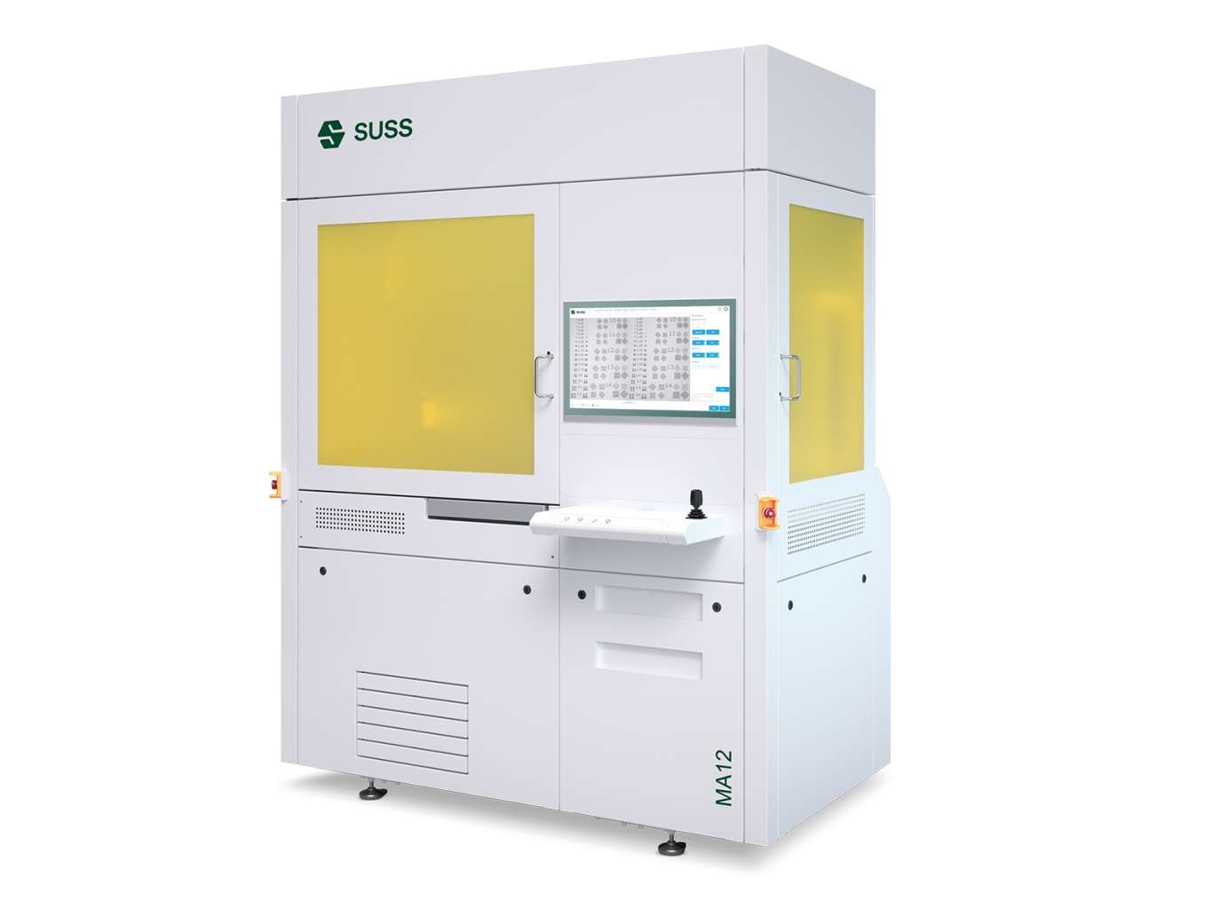
MA100/150e Gen2 Mask Aligner

Dedicated Mask Aligner Solution for High Volume Production of Compound Semiconductors Devices

With the MA100/150e Gen2 SUSS MicroTec has designed a dedicated mask aligner platform for processing high brightness LEDs (HB-LED) on substrates up to 150 mm. With its high precision mask alignment, sophisticated substrate handling for fragile, warped and transparent wafers and its high resolution down to 0.7 µm the MA100/150e Gen2 can overcome all lithography challenges given by the LED manufacturing process. The lowest cost of ownership is achieved by superior throughput performance.

Highlights

  • Dedicated Mask Aligner Solution for HB-LEDs, Power Devices, RF-MEMS etc.
  • Simultaneous handling of 3 wafers allows > 145 wph. incl auto-alignment and exposure
  • Proximity printing for challenging resolution requirements (down to 3 µm L/S at 20 µm exposure gap in thin resist on 100 mm wafer)
  • Multi-size tooling minimizes time required for wafer size changes
  • Non-contact pre-alignment avoids wafer damages
  • The 'Line Alignment' function for sapphire wafers aligns scribe lines precisely to the photo mask
MA100/150e Gen2 Mask Aligner

Based on SUSS MicroTec's production proven mask aligner design the MA100/150e Gen2 enables exceptional process scalability and fast time-to-market for new device designs, while the industry leading throughput of 145 wafers per hour reduces cycle time.

The MA100/150e Gen2 is optimized for wafers sizes up to 6". The system reliably achieves an alignment accuracy of < ±0.7 µm (DirectAlign). Bottom-side alignment (BSA) is optionally available offering an alignment accuracy of < ±1.5 µm. The alignment unit of the MA100/150e is tailored to the specific requirements of LED manufacturing, offering excellent contrast even on transparent and textured wafers.

For applications using scribe lines the new 'Line Alignment' function allows precise alignment of prescribed sapphire wafers to the photo mask without need of traditional wafer targets.

Details : Alignment

  • Top-side alignment (TSA)
  • Bottom-side alignment (BSA)
  • Infrared alignment (IR)
  • DirectAlign®

Details : Exposure

  • Proximity Lithography
  • Soft Contact Exposure
  • Hard Contact Exposure
  • Vacuum Contact Exposure

Details : Exposure Optics

  • MO Exposure Optics®
  • HR and LGO optics
  • Diffraction-Reducing Optics
  • UV-LED light source

Details : Automation

  • Wedge Error Compensation (WEC)
  • Auto Alignment

Details

    Alignment

    • ThermAlign®
    • Large Clearfield Alignment
    • Enhanced Alignment

    Exposure

    • Lab Simulation Software
    • Source Mask Optimization

    Others

    • Wafer Handling Toolings